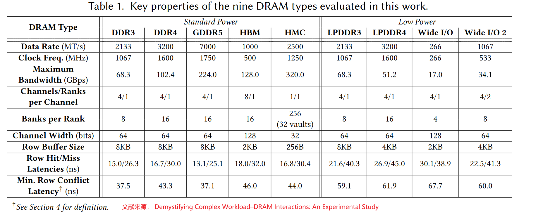
DRAM types: Size, Latency, Bandwidth, Energy Consumption
这篇文章主要聚焦于各种计算设备的DRAM的参数,以及发展趋势。
Situation
DRAM has been a de facto standard for main memory, and advances in process technology have led to a rapid increase in its capacity and bandwidth. In contrast, its random access latency has remained relatively stagnant, as it is still around 100 CPU clock cycles.1

Modern computer systems rely on caches or other latency tolerance techniques to lower the average access latency. However, not all applications have ample parallelism or locality that would help hide or reduce the latency.
Moreover, applications’ demands for memory space continue to grow, while the capacity gap between lastlevel caches and main memory is unlikely to shrink. Consequently, reducing the main-memory latency is important for application performance.
background
- 20-40% of the instructions reference memory2
- compulsory miss rate is 1% or less, caches with more realistic miss rates of 2-10%.
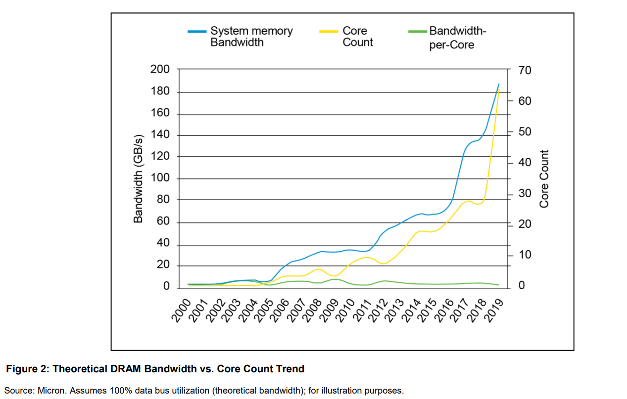
Trend
- DRAM speeds increase by 7% per year, but roprocessor performance is increasing at the rate of 80% per year.
core num VS bandwidth
Motivation: DRAM latency bottleneck
lowering the main-memory latency would benefit many such applications.
Figure 2 shows the relative instructions per cycle (IPC) of SPEC CPU2006 applications when we lower the 28ns access time and the 48ns cycle time of DRAM by 25%, 50%, and 75%.1
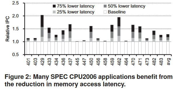
The degree of IPC improvement varies across applications, but an IPC improvement of more than 50% is observed for memory-intensive applications when we cut the DRAM latency by half without changing the bandwidth.
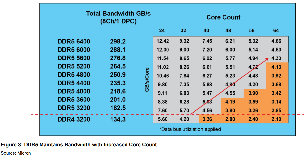
DRAM 设计提速的考虑
- bank-level parallelism(一味的提高会带来 access latency的增加)
Explaination in detail
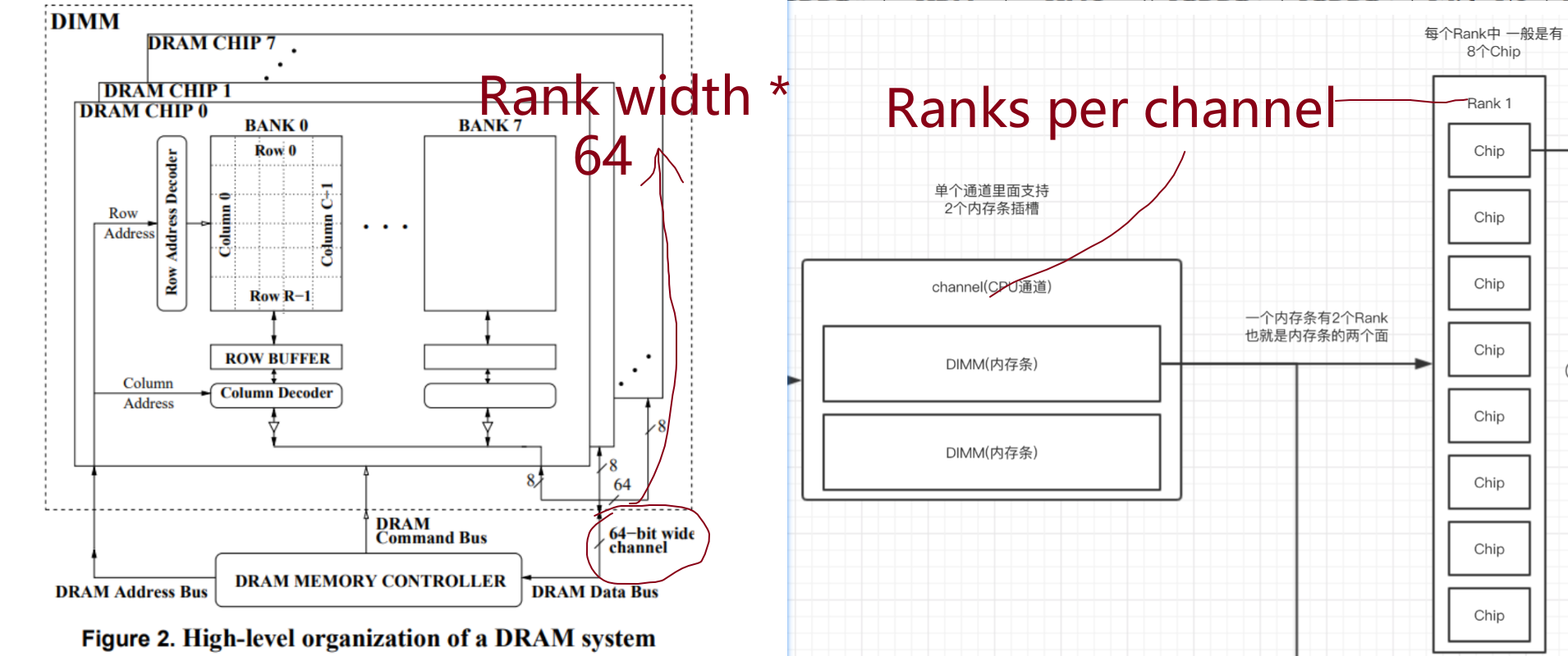
- IO speed = Data Rate
- 单位:
1000 MT/s=1GT/s=1Gbps - IO数 = (ChannelWidth或者 Rank width) * Channels/Ranks per Channel
- Bandwidth = IO speed * IO数 / (8bits/B)
第六行 : 首先 Channel Width应该改成 Rank width
第一二行:由于DDR上下沿的技术(GDDR5 有等效4个上下沿) \(mega transfers per second (MT/s) = 2 * Clock Freq\)
calculation
e.g, \(68.3 GB/s = 2.133GT/s * 64bits * 4 / 8bits/byte\)
\(IO = (ChannelWidth Or Rank width) * Channels/Ranks per Channel\)
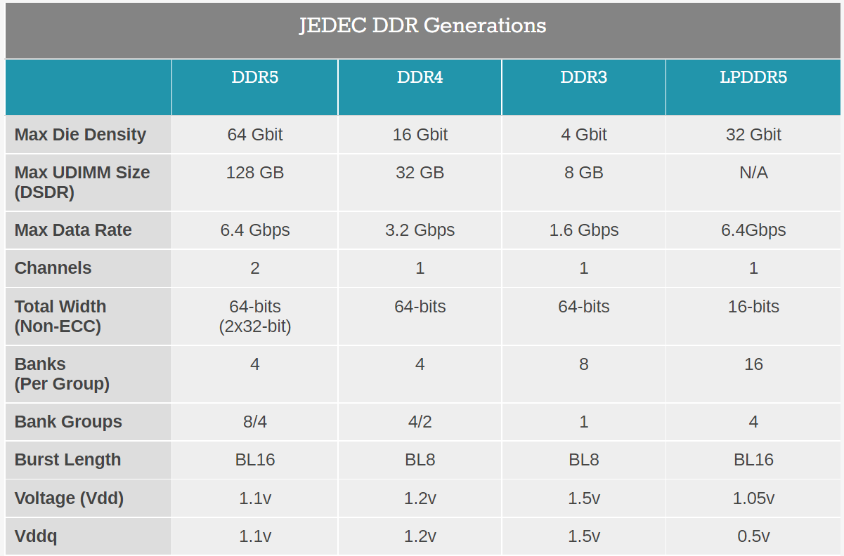
DDR3 DDR4
DRAM 结构
| Feature | DDR3 | DDR4 | DDR5 | LPDDR5 |
|---|---|---|---|---|
| Data rates(Gbps) | 1.6 | 3.2 | 6.4 | 6.4 |
detail diagram
实验室服务器16条32GB的DDR4带宽
Intel(R) Xeon(R) Platinum 8358 CPU 是 Ice Lake 8 通道机器。但是有两个socket的处理器,共同组成16通道。
内存侧 \(3.2 Gbps * 64 bits * 16 / 8 = 409.6GB/s\)
# shaojiemike @ icarus0 in ~ [11:02:13]
$ sudo dmidecode|grep -A16 "Memory Device"|grep "Speed"
    Speed: 3200 MT/s
    Speed: Unknown
    Speed: 3200 MT/s
    Speed: Unknown
    Speed: 3200 MT/s
    Speed: Unknown
    Speed: 3200 MT/s
    Speed: Unknown
    Speed: 3200 MT/s
    Speed: Unknown
    Speed: 3200 MT/s
    Speed: Unknown
    Speed: 3200 MT/s
    Speed: Unknown
    Speed: 3200 MT/s
    Speed: Unknown
    Speed: 3200 MT/s
    Speed: Unknown
    Speed: 3200 MT/s
    Speed: Unknown
    Speed: 3200 MT/s
    Speed: Unknown
    Speed: 3200 MT/s
    Speed: Unknown
    Speed: 3200 MT/s
    Speed: Unknown
    Speed: 3200 MT/s
    Speed: Unknown
    Speed: 3200 MT/s
    Speed: Unknown
    Speed: 3200 MT/s
    Speed: Unknown
实践:查看内存设置
$ dmidecode -t memory|grep DDR4 -A 5 -B11
Handle 0x0025, DMI type 17, 92 bytes
Memory Device
        Array Handle: 0x0006
        Error Information Handle: Not Provided
        Total Width: 72 bits
        Data Width: 64 bits
        Size: 32 GB
        Form Factor: DIMM
        Set: None
        Locator: DIMM350 J70
        Bank Locator: SOCKET 3 CHANNEL 5 DIMM 0
        Type: DDR4
        Type Detail: Synchronous Registered (Buffered)
        Speed: 2933 MT/s
        Manufacturer: Samsung
        Serial Number: 13929A3F
        Asset Tag: 1940
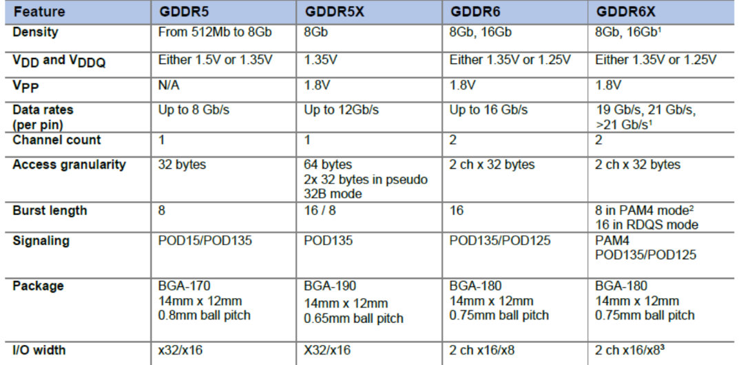
GDDR
| Feature | Graphics DDR5 (GDDR5) | GDDR5X | GDDR6 | GDDR6X |
|---|---|---|---|---|
| Data rates(Gb/s/pin) | 8 | 12 | 16 | 21 |
detail diagram
LPDDR3 and LPDDR4
low-power (LP)
Used in mobile devices
Wide I/O, and Wide I/O 2
also target for low-power devices
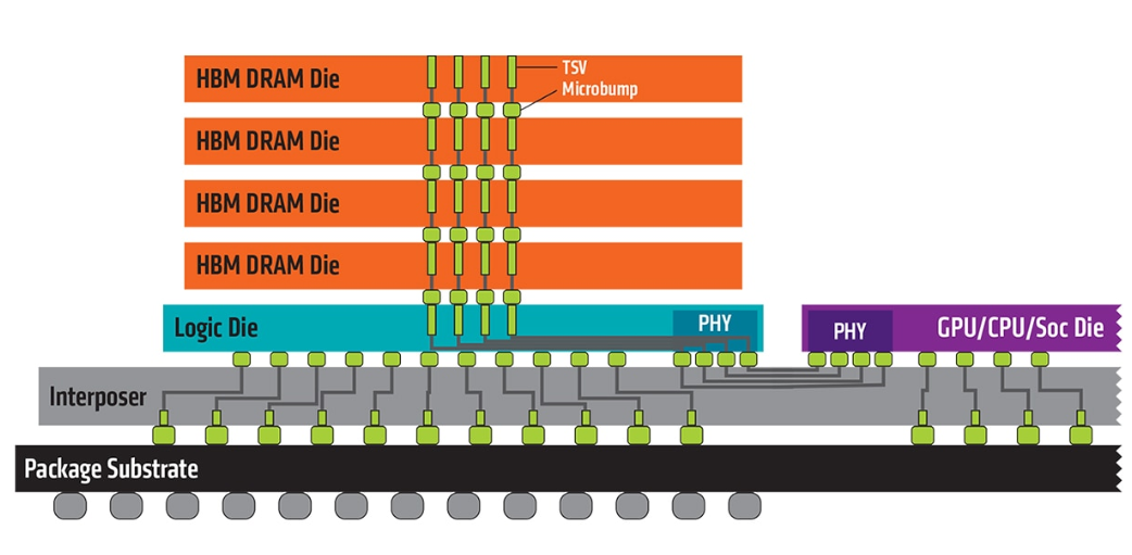
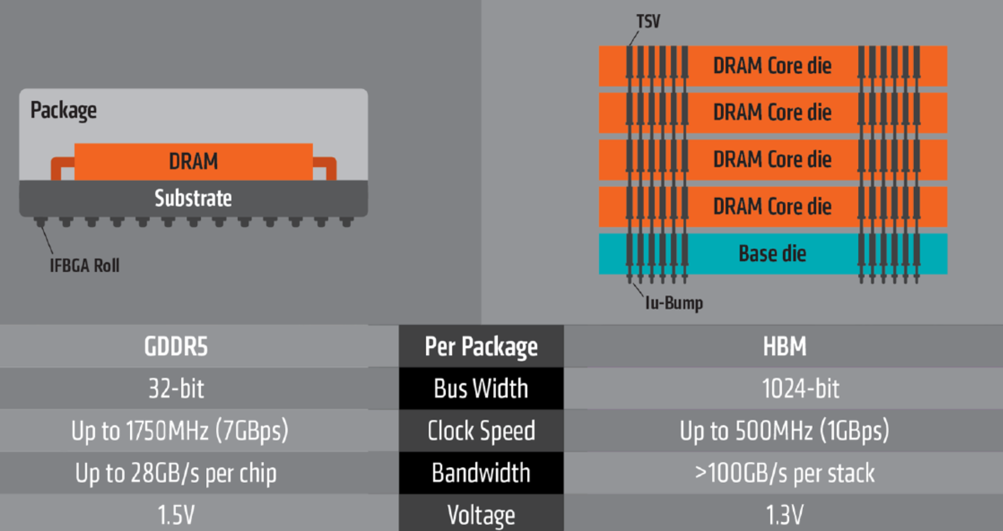
3D-Stacked DRAM
通过多层的DRAM堆叠,through-silicon vias(TSV)和垂直的互联来实现高带宽。
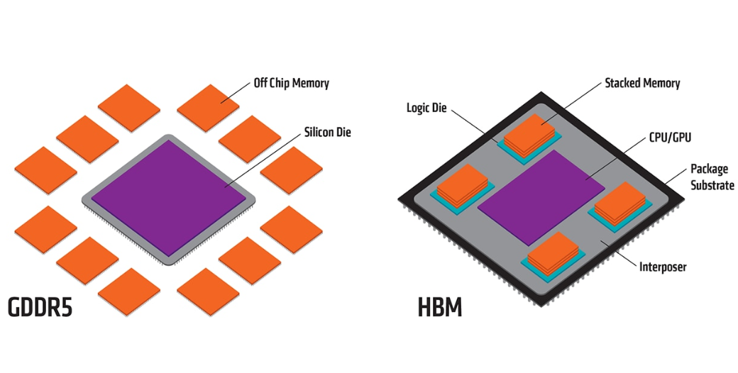
片上集成技术 vs GDRAM
- 节能
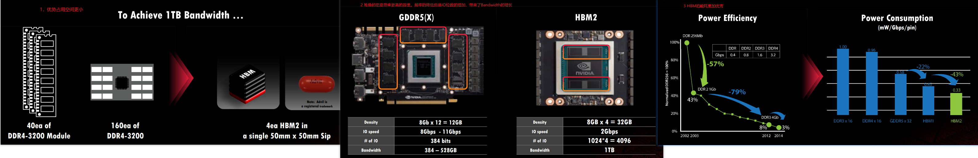
- 传统DRAM 与 soc间的连接数只有 384条。为了提高性能只能提高频率
- 与传统的GDDR内存相比,GDDR依赖于较窄的接口(例如,GDDR6通常使用16或32位的接口宽度),但运行在更高的时钟频率下。HBM通过这些众多的并行通道能够在相对较低的时钟频率下工作,从而实现高带宽的同时降低功耗。
- 频率的增加带来的是巨大的功耗增加
- 高带宽,片上集成能大大增加连接数(HBM 1 stack 1024 I/O)
- 频率也不需要那么高(3.2Gb/s/pin)
- 随着HBM3达到(9Gbps/pin)接近GDDR6x(16/18Gbps/pin)。HBM的总带宽开始反超
HBM 内存相对于GDDR的优势在哪里?
HBM(High Bandwidth Memory)内存和GDDR(Graphics Double Data Rate)内存是两种不同类型的内存技术,它们在性能、结构和应用方面有着明显的差异。相对于GDDR内存,HBM内存的优势主要体现在以下几个方面:
-
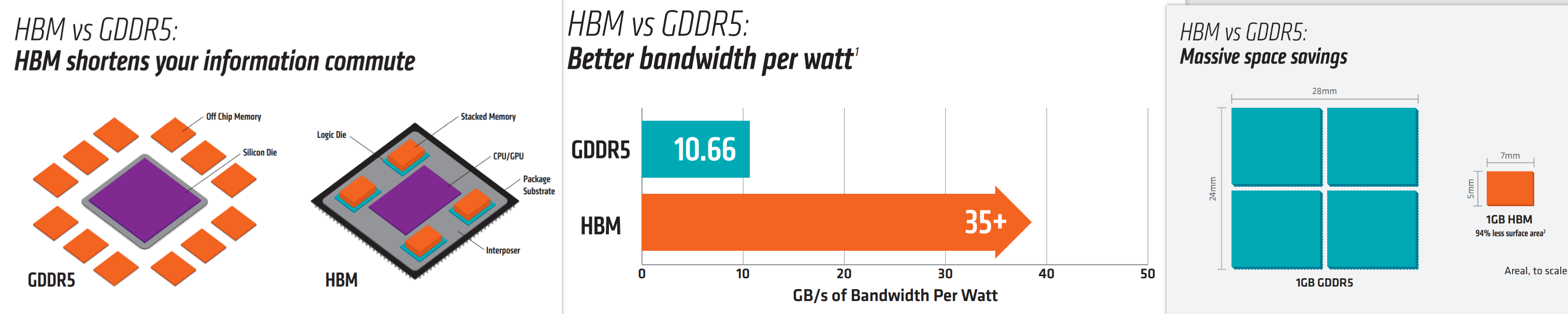
更高的带宽:HBM内存使用一种堆叠的3D芯片设计,通过宽接口并行传输数据,能够提供远高于GDDR内存的带宽。这使得HBM非常适合带宽要求极高的应用,如高性能计算、深度学习和高端图形处理。
-
更低的功耗:HBM内存通过接口的设计优化,以较低的电压运行,并且因为信号传输距离短,减少了能量消耗。相比之下,GDDR内存通常需要更高的电压和更长的信号传输路径,这会导致更高的功耗。
-
更紧凑的封装:由于HBM内存采用的是堆叠芯片设计,它可以在相对较小的物理空间内提供更多的存储容量和带宽。这种紧凑的封装方式使得HBM非常适合空间受限的应用场景,如移动设备和紧凑型PC。
-
更低的延迟:HBM内存由于其独特的堆叠设计和近距离的芯片间通信,能够实现更低的数据访问延迟,这对于需要快速数据访问的应用来说是一个重要优势。
-
热效率更高:HBM的堆叠设计有助于更有效地分散热量,这与较高的能效相结合,使得整体热管理更为高效,对于需要维持低温度的高性能计算环境尤为重要。
然而,这些优势通常伴随着更高的成本,因为HBM内存的制造过程更为复杂,并且需要更精密的技术来实现堆叠和互连。此外,HBM的生产成本和技术门槛也比GDDR更高。因此,HBM内存主要用于高端市场,而GDDR内存由于成本效益较高,更普遍应用于主流图形卡和游戏设备中。
HBM 宽接口的原因
我觉得是On-chip的HBM,能相对于Off-Chip的GDDR做更多的片上IO。
HBM(High Bandwidth Memory)的宽接口设计是它能够提供高带宽的关键特征之一。这种设计之所以采用,主要是基于以下几个原因:
- 3D堆叠技术:HBM利用了3D堆叠技术,将多个内存层物理地堆叠在一起,并通过硅通孔(TSVs,Through-Silicon Vias)和微凸块(microbumps)在这些层之间建立电连接。这种堆叠方式大幅减少了信号传输距离,允许更多的数据通道在堆叠的层之间并行工作,从而实现宽接口。
- 并行数据传输:HBM的宽接口允许它同时传输大量数据,这是通过将数据分散到成百上千的独立数据通道上来实现的。与传统的GDDR内存相比,GDDR依赖于较窄的接口(例如,GDDR6通常使用16或32位的接口宽度),但运行在更高的时钟频率下。HBM通过这些众多的并行通道能够在相对较低的时钟频率下工作,从而实现高带宽的同时降低功耗。
- 降低功耗:宽接口使得HBM可以在较低的时钟频率下运行,这减少了每比特传输的能量消耗。较低的时钟频率意味着对电源和冷却需求较低,有助于提高整体能效比。
- 提高空间效率:由于HBM内存堆叠在处理器或GPU旁边,它的宽接口设计有助于减少占用的板载空间。这对于空间受限的应用(如移动设备、紧凑型PC或高性能计算系统)尤为重要。
- 减少IO复杂性:宽接口还有助于简化内存控制器的设计,因为它减少了对极高速序列接口的需求,这些接口通常需要更复杂和成本较高的信号完整性解决方案。
总的来说,HBM的宽接口设计是一种平衡高带宽、低功耗和空间效率的方法,尽管这种设计增加了制造复杂性和成本,但它为高性能计算和图形处理提供了显著的性能优势。
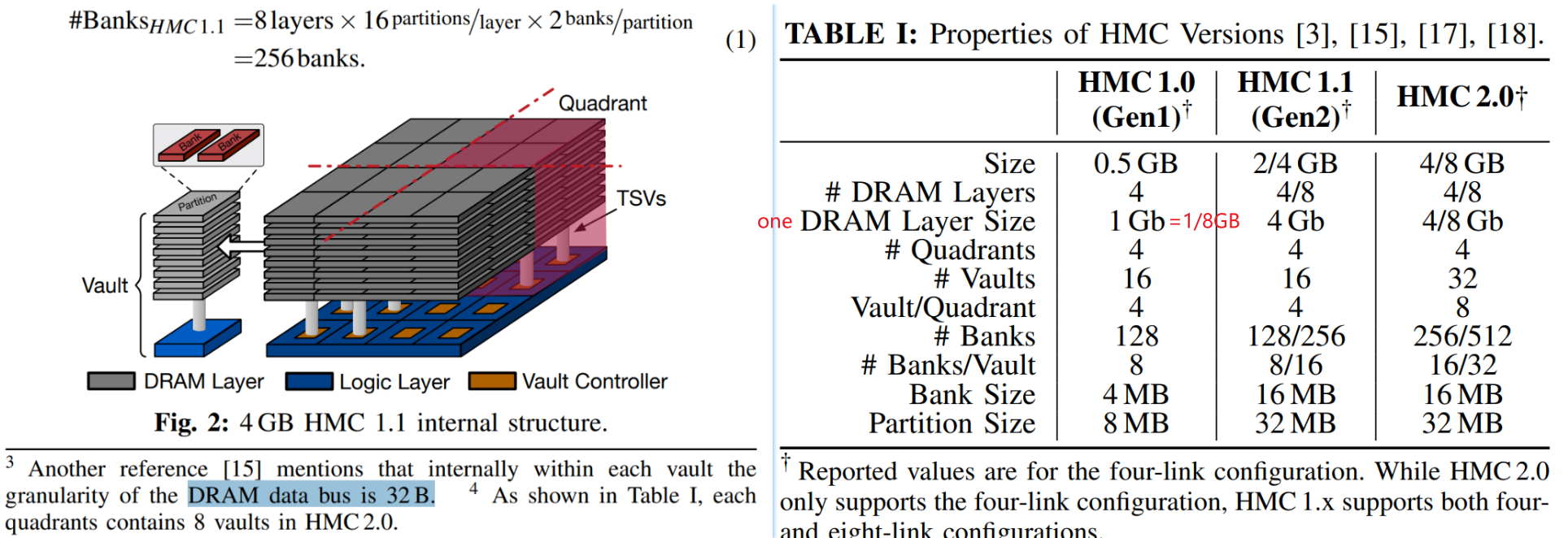
Hybrid Memory Cube (HMC)
MICRON(美光)于2011年推出的
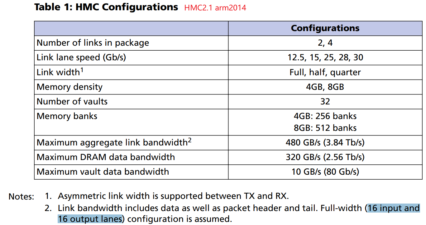
Bandwidth detail
- Maximum vault data bandwidth
10 GB/s(80 Gb/s) - quadrant, whose vaults share a single external link.
- each external link is a 16- (full-width) or eight-lane (half-width) connection that supports full-duplex serialized communication across each bit lane with configurable speeds of 10, 12.5, or 15 Gbps.
- a eight-link full-width HMC device whose link operates at 15 Gbps has a maximum bandwidth of
\(8link×16lanes/link×15Gbps×2 full duplex = 480GB/s\)
有几个显著的特点
- 为了增大并行性,采用了更多的banks数(256个在HMC v2.1).但是带来了延迟的增加
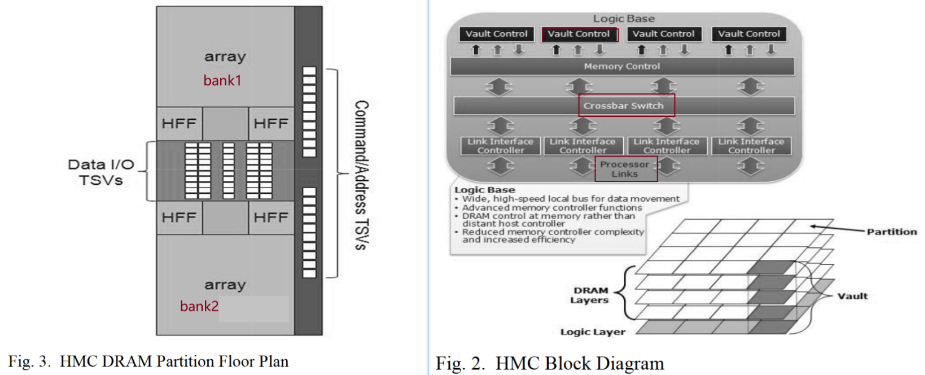
- 将memory controller(i.e., vault controller)集成到logic layer,相互之间通过network-on-chip (NoC)连接。CPU只需要发送FIFO的requests就行。
- 为了方便管理logic,将其划分成vaults。每个由许多垂直的memory切片组成。为了实现这点,memory(page size还是行大小)由4-8kB变成256bytes(导致 spatial locality 不好,重复密集访问?)
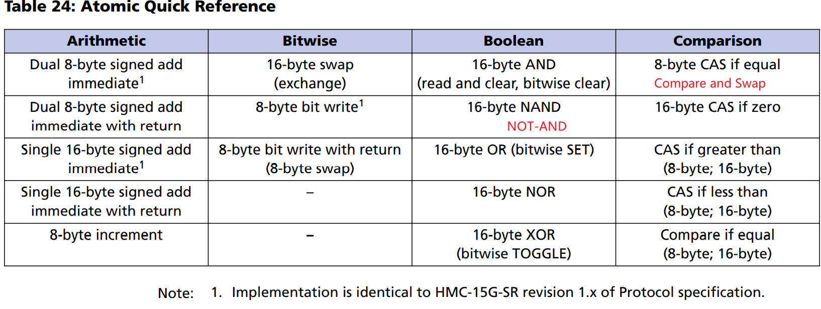
HMC2.1
HMC2.1的Atomic Request Commands
Atomic requests 从DRAM读取 16bytes(由request ADRS/address确定), 对数据进行一次16位命令的操作之后,写回DRAM的相同位置。
The read-update-write sequence occurs atomically, meaning that subsequent requests to the same bank are scheduled after the write of the atomic request is complete
HMC与DDR的区别
Many of the traditional functions found in a DRAM have been moved to the logic layer, including the high-speed host interface, data distribution, address/control, refresh control and array repair functions
HMC与HBM的区别
- HBM are limited in terms of scalability and bandwidth which is due to their wide buses and the use of the standard DDRx protocol.
- HMC: a generation of 3D-stacked memories with packet-based communication has been introduced and is currently implemented in the Hybrid Memory Cube. The HMC interface utilizes a packet-based communication protocol implemented with high speed serialization/deserialization (SerDes) circuits.
High Bandwidth Memory (HBM)
Advanced Micro Devices(AMD) 2013年提出的技术(SK海力士 (SK Hynix)貌似也有参与):目标是提升GPU的带宽,频率虽然低于GDDR5,但是采用了更多的four to eight memory channels
现在是HBM3
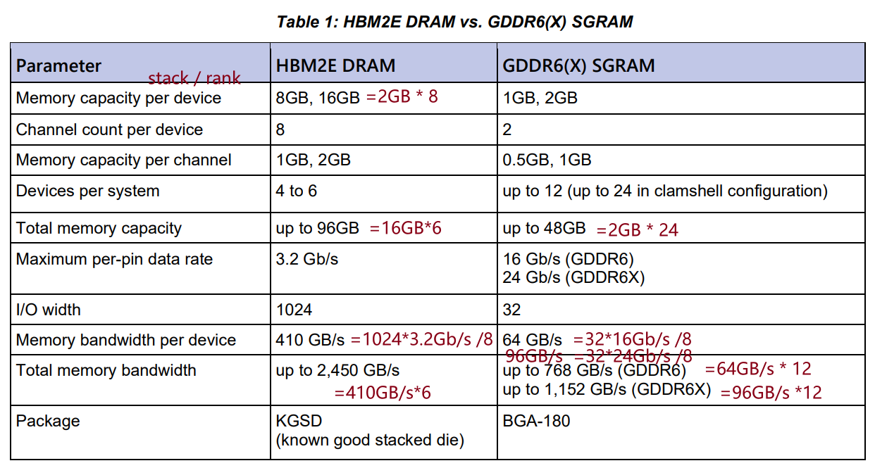
HBM2e
micron的标准
- 速度:3.2Gbps
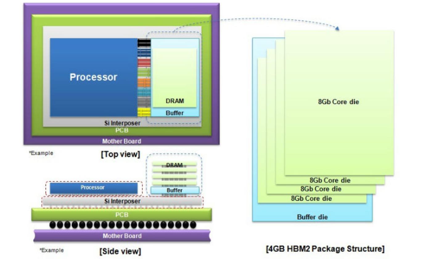
410GB/s. - 大小:16GB / die
基本结构参数
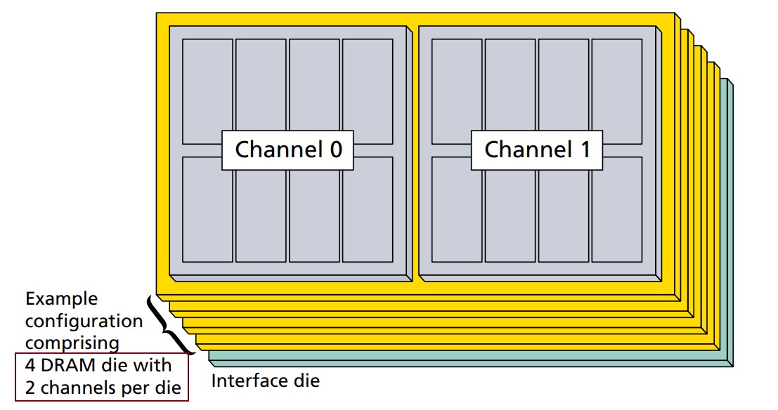
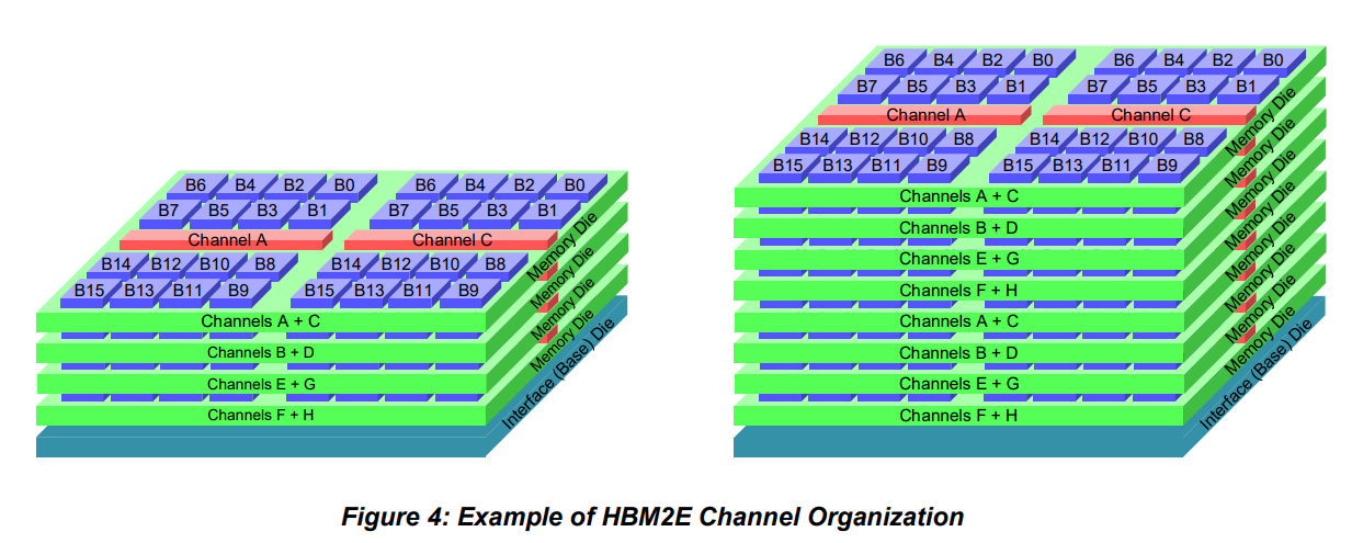
The division of channels among the DRAM die within a stack is irrelevant to the memory controller. The example above, with the memory for two channels implemented on each die, is not a required organization.
Because each channel is independent。 A channel provides access to a discrete pool of memory. Channels are individually clocked and need not to operate synchronously.
Channel Architecture
无论是8GB还是16GB的,都是A-H共8个channel。各自的command/address, clock, data interface。 8层的HBM只是将每个channel的大小扩大一倍。
HBM3
SAMSUNG的标准
- 速度:6.4Gbps
819GB/s. - 大小:HBM3 Icebolt堆叠12层10 nm级16 Gb DRAM芯片,可提供
24GB内存
HBM与GDDR的区别
以实际产品的参数比较举例
Nvidia 历代计算卡使用HBM
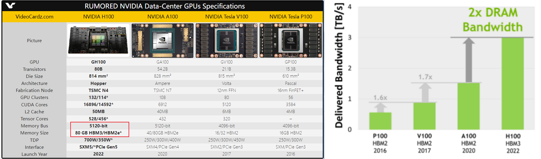
H100显存只用了五颗,最新一代HBM3,容量80GB(16*5),位宽5120-bit,带宽高达3TB/s,相比A100多了一半。
IO Speed = \(3*1024*8/5120 = 4.8 Gbps\)
HBM vs GDDR5
 <!--
<!-- 
 -->
Compared to GDDR5, HBM can fit the same amount of memory in 94% less space!
-->
Compared to GDDR5, HBM can fit the same amount of memory in 94% less space!
HBM3 vs GDDR6X
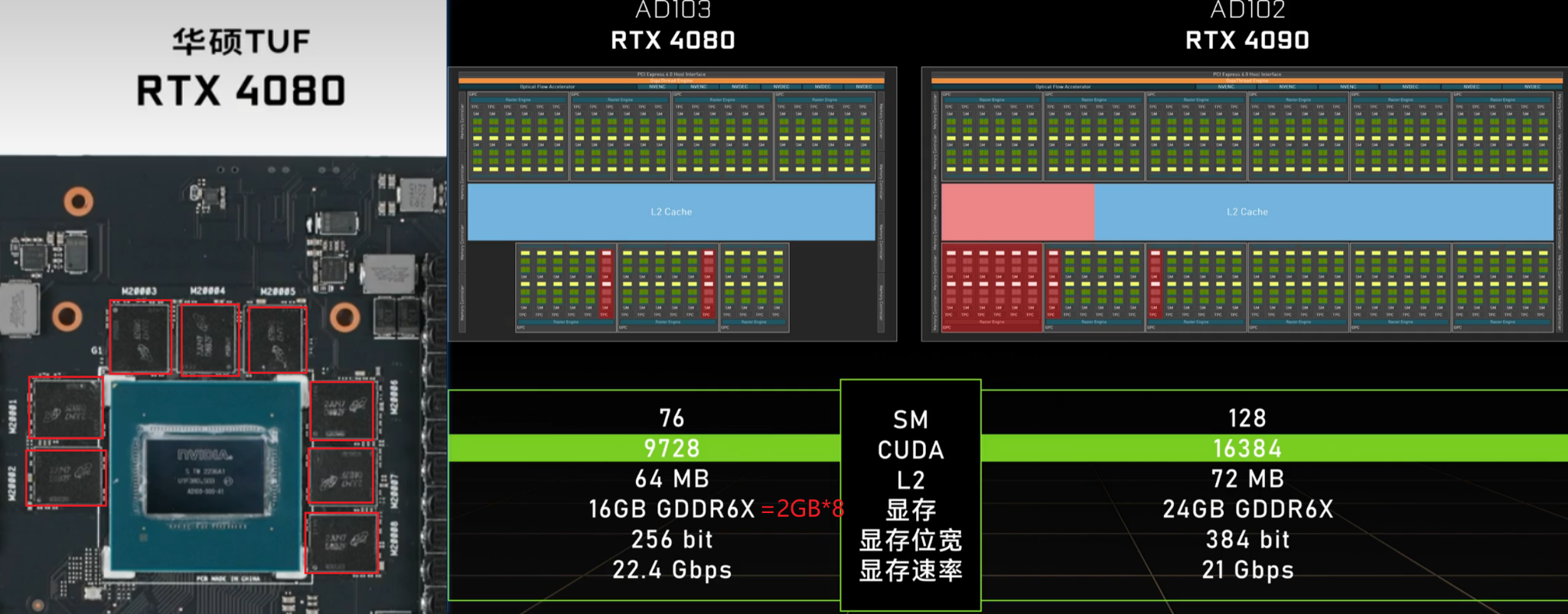
4090(GDDR6X) 带宽 = \(21 * 384 /8 = 1008 GB/s\) << H100(HBM3) 3TB/s
4080(GDDR6X) 带宽 = \(22.4 * 256 /8 = 716.8 GB/s\)
参考文献
https://www.amd.com/system/files/documents/high-bandwidth-memory-hbm.pdf
https://www.micron.com/-/media/client/global/documents/products/data-sheet/hmc/gen2/hmc_gen2.pdf
-
ISCA'13 Reducing Memory Access Latency with Asymmetric DRAM Bank Organizations ↩↩
-
Hitting the Memory Wall: Implications of the Obvious ↩
-
ISPASS'18 Performance Implications of NoCs on 3D-Stacked Memories: Insights from the Hybrid Memory Cube ↩
-
S. Ghose, T. Li, N. Hajinazar, D. Senol Cali et al., “Demystifying Complex Workload-DRAM Interactions: An Experimental Study,” in SIGMETRICS, 2019. ↩